A research group led by Associate Professor Yu Yi from the School of Physical Science and Technology (SPST), ShanghaiTech University, in collaboration with teams from Purdue University and the University of Science and Technology of China, have made a significant breakthrough in fabricating patterned lateral heterostructures in two-dimensional (2D) halide perovskites. The study was published online on January 14 in Nature under the title “Mosaic lateral heterostructures in two-dimensional perovskite.”
Lateral heterostructures—structures where different materials are joined side-by-side—are crucial for exploring exotic physics, creating new devices, and enabling miniaturization. However, 2D lead halide perovskites have proven difficult to pattern because of their “inherently soft and unstable ionic lattice,” making conventional lithography and etching too destructive.
This study developed a gentle new approach: in a liquid environment, the two-dimensional ultrathin layered perovskite material spontaneously “etches” to form square holes of controllable size. These holes then serve as “molds” for growing another type of perovskite material inside, resulting in mosaic-like lateral heterostructures—seamless splicing of different materials. Understanding how this spontaneous etching occurs is crucial for improving the method and future applications. To figure it out, it is necessary to directly observe the atomic-scale structure of the etched holes. Unfortunately, perovskite materials easily collapse or decompose under the electron beam irradiation of conventional electron microscopes, making it difficult for standard methods to obtain reliable images.
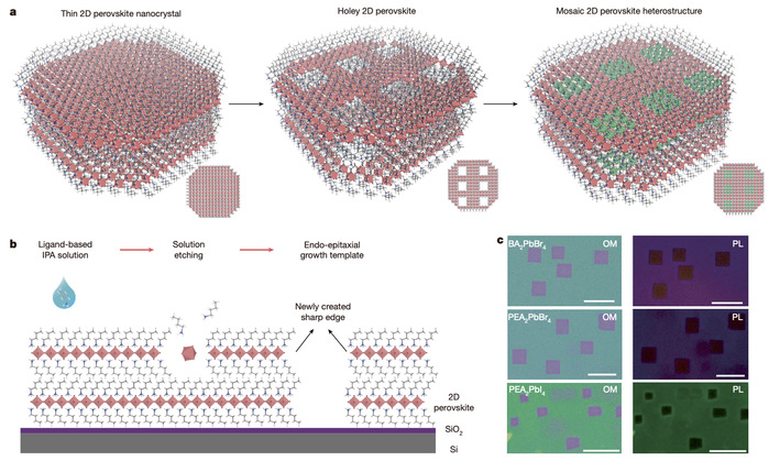
Schematic of the fabrication of holey 2D perovskite and the mosaic lateral heterostructures in 2D perovskite
The Yu team adopted low-dose high-resolution transmission electron microscopy (HRTEM) technology, successfully comparing the atomic arrangements near the holes before and after etching. They discovered that the internal strain, pressure from stretching or compression, in the material is the key factor triggering the etching. Once etching begins, the holes stably grow along specific crystallographic directions of the perovskite crystal ([100]/[010] directions), forming neat squares. Further observations also proved that the other perovskite material grown inside these holes can perfectly match the lattice with the original material, forming high-quality epitaxial structures.
This achievement will provide a universal material platform for developing complex integrated light-emitting devices, such as more advanced LED displays or sensors. Particularly noteworthy is that the Yu team’s original low-dose HRTEM method offers important scientific inspiration for deeply understanding the intrinsic structural characteristics and structure-property relationships of halide perovskites.
Lu Yuan PhD ’25 from the SPST is the co-first author of the paper. Prof. Yu Yi is the corresponding author.