A joint research team led by Associate Professor Yu Yi from the School of Physical Science and Technology (SPST) at ShanghaiTech University, in collaboration with the University of Antwerp and Purdue University, has achieved a major breakthrough in electron microscopy studies of radiation-sensitive materials. Using low-dose electron microscopy imaging, they succeeded in revealing the atomic-scale structure of edges and defects in halide perovskite materials for the first time. The findings were published online in an article entitled “Atomically Resolved Edges and Defects in Lead Halide Perovskites” in the academic journal Nature on October 29 (Beijing Time).
Since the advent of electron microscopy, atomic-scale imaging of radiation-sensitive materials has remained a significant challenge in the field of microscopy. Across both life sciences and materials science domains, substances composed of light elements, possessing weak atomic bonding energies or high chemical reactivity, undergo rapid structural collapse and chemical decomposition under electron beam irradiation. This characteristic not only impedes the acquisition of atomic-resolution images but also severely constrains the in-depth understanding of such materials’ microstructure and physical and chemical properties.
Currently well-studied and widely applied material systems, ranging from traditional steels to modern silicon-based semiconductors, exhibit superior tolerance to electron beam irradiation. This key property has enabled researchers to thoroughly observe and precisely analyze microscopic defect structures, providing crucial support for theoretical research and process optimization in materials science, thereby effectively advancing technological innovation and engineering applications in the field. In contrast, certain new energy materials demonstrate exceptional sensitivity under electron radiation, with halide perovskites being a prominent example.
As a novel optoelectronic functional material system, halide perovskites demonstrate significant promise for energy conversion applications such as solar cells. However, stability issues severely hinder their industrial-scale deployment, as they readily degrade under atmospheric exposure while also exhibiting inadequate stability during device operation—both contributing to rapid performance deterioration. Fundamental principles of materials science indicate that microscopic defects within crystal structures constitute energetically unstable regions that serve as critical sites for triggering structural transformations and performance degradation. Therefore, atomic-scale characterization of defect features in halide perovskite materials holds decisive significance for elucidating structure-property relationships and guiding material design.
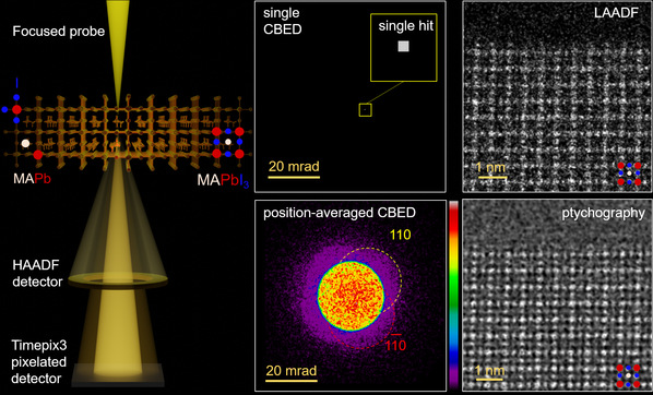
This research has achieved atomic-resolution electron ptychography imaging under the lowest electron dose conditions to date by employing an ultralow-dose four-dimensional scanning transmission electron microscopy (4D-STEM) with dose fractionation. Not only does this mark the first observation of complete atomic configurations at halide perovskite edges, but it also captures their dynamic structural evolution. Experimental findings reveal that the edges of organic-inorganic hybrid methylammonium lead iodide perovskite (MAPbI3) predominantly exhibit methylammonium (MA) and iodine (I) termination structures. Furthermore, the damage rates at both edges and internal defects show a strong correlation with the concentration and types of vacancies. Notably, high concentrations of iodine vacancies demonstrate a significant correlation with accelerated degradation processes.
Postdoctoral Researcher Yuan Biao PhD ’22 at the University of Antwerp, Wang Zeyu ’19, PhD ’24, and Professor Zhang Shuchen at the University of Science and Technology of China (USTC) are the co-first authors of the paper. Professor Dou Letian at Purdue University, Professor Yu Yi, and Professor Timothy Pennycook from the University of Antwerp are the co-corresponding authors. The sample synthesis and preparation were conducted by research teams from Purdue and USTC. The electron microscopy data acquisition and non-iterative electron ptychography analysis were performed by the Antwerp team, and the iterative low-dose electron ptychographic reconstruction was completed by ShanghaiTech team. Professor Han Yu from South China University of Technology also contributed to this research.