A recent study offers a promising step toward improving the performance of silicon-based photonic devices, which are key components in modern optics, communications, and quantum technologies. This study was conducted by the team led by Assistant Professor Shen Xiaoqin from the School of Physical Science and Technology (SPST) at ShanghaiTech University. By applying an ultra-thin molecular layer to a common photonic material, the researchers significantly boosted the efficiency of light conversion processes, potentially bridging integrated photonics with existing chip manufacturing methods. Their work was reported in Opticain an article titled “Molecule-induced surface second-order nonlinearity in an inversion-symmetric microcavity.”
The problem: silicon’s hidden limitation
Silicon photonics—the technology behind advanced LiDAR and future optical computing—relies on manipulating light. However, silicon and related materials, such as silica and silicon nitride, inherently lack a key property called second-order nonlinearity, which is essential for tasks such as frequency conversion (converting light to different frequencies) or generating quantum light. For decades, researchers have struggled to overcome this limitation without resorting to complex and costly materials that are not compatible with standard silicon chip manufacturing.
The innovation: a molecular “upgrade”
The research team addressed this challenge by applying a monolayer of specially designed molecules—just 1.2 nanometers thick, roughly 1/100,000th the width of a human hair, to the surface of a silica microcavity, a sphere-shaped structure that traps and amplifies light. These molecules, arranged asymmetrically, unlocked the device’s ability to convert infrared laser light into visible light through a process called second harmonic generation (SHG). Under low-power laser light (similar to telecom systems), the coated device produced visible light with 100 times greater efficiencycompared to uncoated versions. Supported by theoretical modeling, the team discovered the enhancement, which stems from interactions between the laser’s evanescent field (light that extends beyond the microcavity’s surface) and the molecular layer.
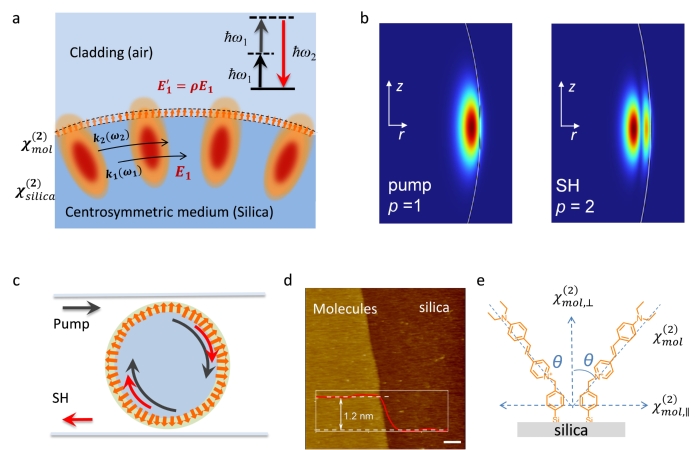
Figure 1. The theoretical model of molecular strategy for boosting second-harmonic generation
“The molecular layer can be applied to existing silicon photonic components such as silica, silicon, and silicon nitride, using standard fabrication techniques,” Shen said. “The relative simplicity of the fabrication and molecule-coupling approach could be applied to mass production in typical complementary metal-oxide semiconductor (CMOS) foundries.”
While still in the experimental stage, the research team notes that this proof-of-concept study provides a blueprint for enhancing silicon-based integrated photonics without overhauling current manufacturing processes, thereby helping meet growing demands for higher-efficiency, lower-cost, and more energy-efficient technologies.
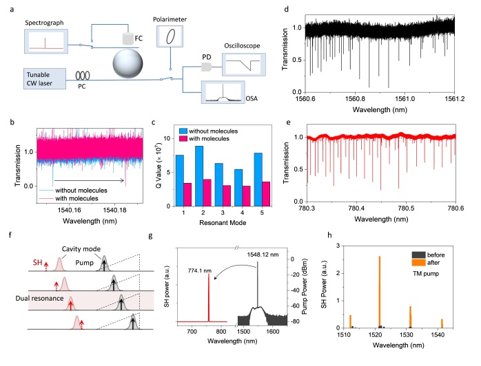
Figure 2. Optical setup, device’s characteristics, and SHG performance
SPST alumni Wang Ru and Dai Yue are the co-first authors, and Prof. Shen is the corresponding author. ShanghaiTech is the sole affiliation.
*This article is provided by Prof. Shen Xiaoqin