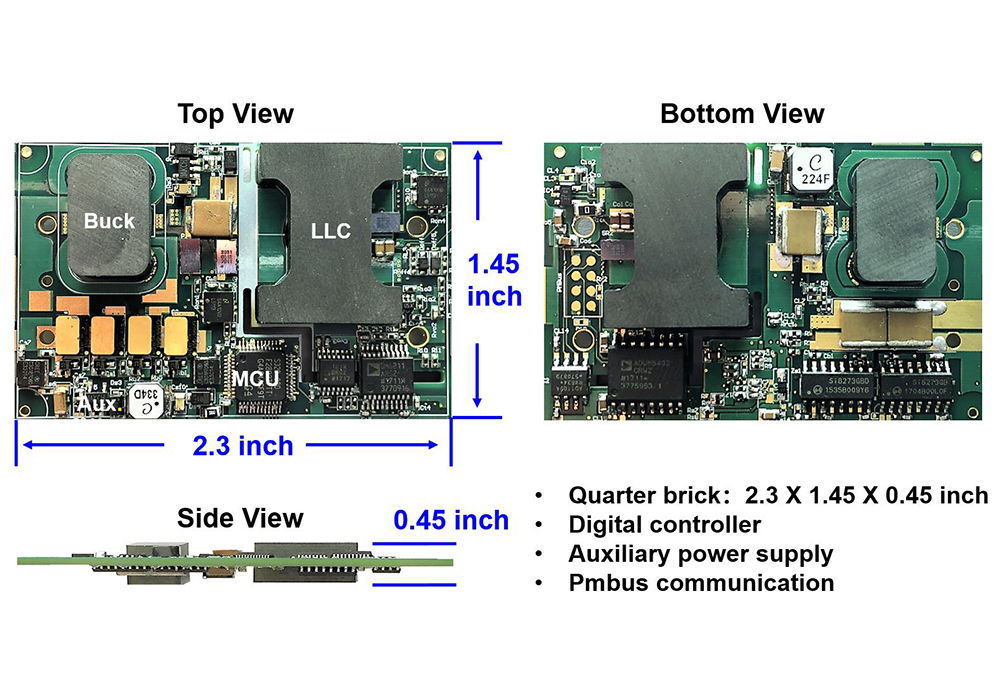
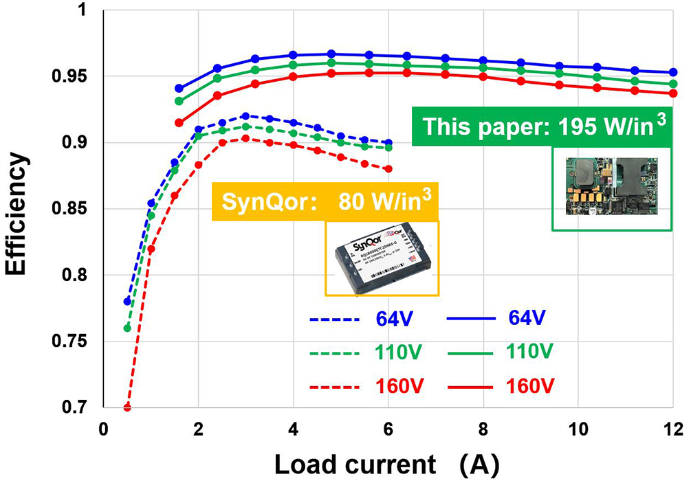
Recently, SIST Assistant Professor Fu Minfan proposed a 300W 110V/24V digital DC/DC module based on gallium nitride (GaN) devices. The proposed module can achieve 95.8% peak efficiency and 195 W/inch3 power density, which are much better than the state of the art (Synqor’s module: 91% peak efficiency and 80 W/inch3 power density). Recently, his work on magnetic design and high-frequency digital control were published in IEEE Transactions on Power Electronics and IEEE Transactions on Industrial Electronics respectively.
The increased power consumption and power density demands of modern technologies have increased the demands on various power supplies. Combined with focus on global energy savings and size reduction, there are continuous research efforts on developing high efficiency and high power density converters. Currently, most of the commercial converters are still based on silicon (Si) devices. It is difficult to further improve the efficiency and power density because the Si-based semiconductor devices approach their theoretical performance limit. The emerging wide-band-gap (WBG) device, such as gallium nitride (GaN) device will certainly become the game changer because of its better figure-of-merit and significantly smaller body diode reverse-recovery effect. In order to fully utilize the benefits of GaN device, there are still many challenges in device and topology selection, converter configuration, modeling and control, and magnetic design.
The research developed a wide-input-range (64V-160V to 24V) rail grade dc/dc converter based on GaN devices and proposed a two-stage configuration, as shown in Fig.1. The first regulated stage was a two-phase interleaved buck converter (>400kHz) and the second unregulated stage was a LLC (2 MHz) dc transformer. In order to achieve high frequency and high efficiency, the critical mode operation was applied for the buck converter, and the negative coupled inductors were used to reduce the frequency and the conduction losses. Then Fu proposed a systematical methodology to optimize the planar coupled inductors. For the unregulated LLC converter, it can always work at its most efficient point and an analytical model was used to optimize the planar transformer.
The work was published in IEEE Transactions on Power Electronics (early access) with the title, “Optimal Design of Planar Magnetic Components for A Two-Stage GaN-Based DC/DC Converter” and IEEE Transactions on Industrial Electronics (early access) with the title,“A GaN-Based DC/DC Module for Railway Applications: Design Consideration and High-Frequency Digital Control.”The work was a collaboration between Dr. Fu Minfan and Virginia Tech Dr. Fred C. Lee’s research group Center for Power Electronics Systems (CPES). The first author for both papers was Dr. Fu Minfan. The work was supported by CPES-CRRC collaboration funding and start-up funding from ShanghaiTech.
Read more at: https://ieeexplore.ieee.org/document/8392748
Read more at: https://ieeexplore.ieee.org/document/8635503

Fig. 1:Proposed two-stage topology.

Fig.2:Prototype.

Fig.3:Comparison with the state of the art.

