Under the guidance of Assistant Professor Feng Jicheng in the School of Physical Science and Technology (SPST), a research team has recently made a significant contribution to the fabrication of complex architectures at the nanoscale. Their findings, published in the journal Advanced Functional Materials in March and featured as the journal’s back cover, introduced an innovative 3D nanoprinting technique. This novel approach utilizes electric fields as nanoscale drawing tools, achieved by electrically biasing three parallel planes, with the central plane featuring periodic perforations. By manipulating the potentials applied to these planes, the team has demonstrated the programmable assembly of charged nanoparticles into precise nanoscale metallic arrays. This groundbreaking technology is anticipated to surpass current limitations on feature size and spacing, paving the way for the integration of a greater number of devices onto a single chip.
Back cover: Three plates enabling the printing of nanomaterials in 3D
Fundamental differences and key innovations
The fabrication of integrated circuits (ICs) is a cornerstone of modern nanoengineering, where the reduction in component size and increased packing density are critical for enhancing computational power. Traditional IC fabrication predominantly relies on lithographic processes, a subtractive manufacturing method limited by the wavelength of the light source, constraining achievable feature sizes. In contrast, Feng’s groundbreaking research introduces an addictive manufacturing approach by employing electric fields for the nanoscale printing of metals, diverging from optical systems (see Figure 1). This method uses electrically biased planes to generate electric fields that can print nanoarchitectures at high precision over a large area. The proposed fabrication method showcases a significant departure from previous 3D printing techniques that relied on unstable gaseous ionsto modify electric fields topographies.
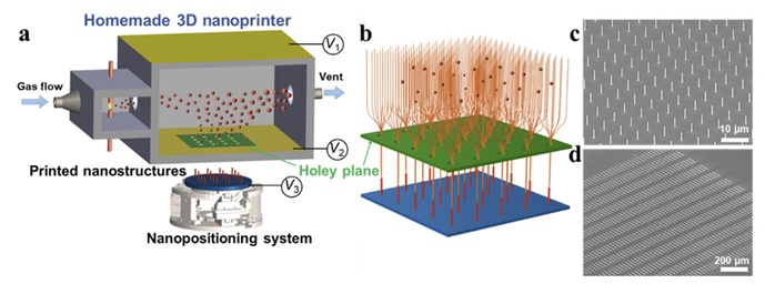
Figure 1. Schematic of the 3D nanoprinting setup.
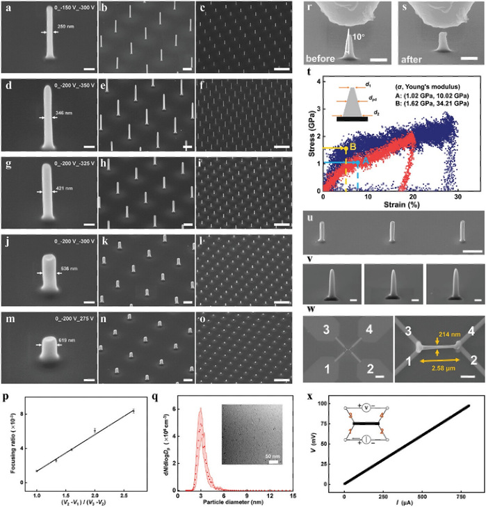
Figure 2. Programmable and parallel 3D nanoprinting for fabricating metal nanopillars with excellent mechanical and electrical properties.
The newly developed 3D nanoprinter leverages three horizontally aligned parallel plates, with the middle plate featuring a pattern of micron-sized holes, all subjected to electrical biasing. By fine-tuning the potentials applied to these plates, the differences in electric field strength create a funnel-like configuration through the periodic holes (see Figure 2). Notably, the width of this ‘electric funnel’ can be precisely controlled, consuming merely ~1% of the hole size, suggesting the potential for reduction to atomic scale widths through careful potential adjustments. This capability significantly surpasses the resolution limits of wavelength-dependent lithographic techniques and heralds a new era in nanoprinting by enabling the assembly of atomic clusters individually. By mobilizing the substrate, the density of printed features can be increased, and the printing area can also be enlarged (see Figure 3).
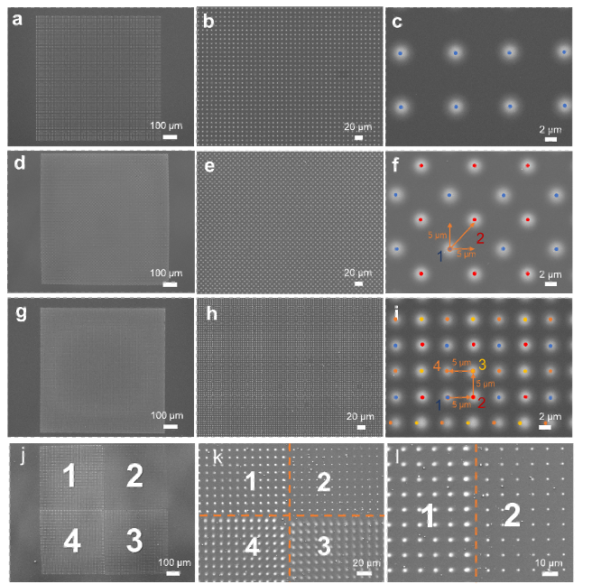
Figure 3. Structure densification and the enlargement of the printing area.
This 3D nanoprinting approach not only facilitates a highly predictable strategy for particle assembly but also synergizes with traditional photolithographic methods, enhancing various aspects of IC fabrication. This versatile nanoprinter can create 3D architectures of hard materials across large areas, with feature sizes adjustable from ~10 to 750 nm “on the fly”. The compatibility of 3D nanoprinter with a broad range of metals (such as Pt, Au, Ag, Pd, Cu) and semiconductors (such as Si and Ge), alongside the system’s digitalization through computerized potential adjustments to each plane, offers unprecedented precision and flexibility.
By transitioning from subtractive to additive manufacturing, Feng’s work paves the way for achieving smaller feature sizes and pitches beyond the limitations of conventional photolithography, opening new avenues for research and application in the fields of nanoelectronics and nanophotonics. This advancement not only showcases the potential for further miniaturization but also invites the scientific community to validate, refine, and leverage this technique for future breakthroughs.
All the authors are solely affiliated to ShanghaiTech University. Among others, Liu Shirong, the first-year PhD student in SPST, is the first author of the paper, and Prof. Feng Jicheng is the corresponding author.
*This news article is provided by Prof. Feng Jicheng and edited by ShanghaiTech Global